| Blog Icon | Blog Title | |
|---|---|---|
|
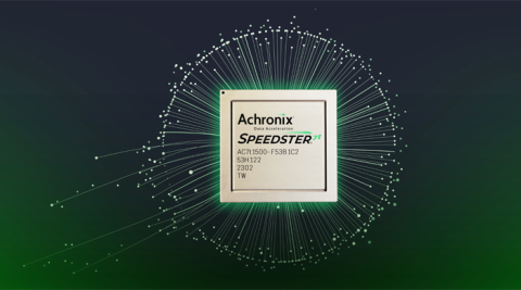
Accelerating LLM Inferencing on FPGAs– Bob Siller,Director, Product MarketingHow do Speedster7t FPGAs stack up against GPU solutions when running the Llama2 70B parameter model? The evidence is compelling — Achronix Speedster7t FPGAs outperform in processing LLMs by delivering an optimal combination of computational power, memory bandwidth, and exceptional energy efficiency. |
> |
|
Achronix Achieves up to 300% Improvement in SoC Verification Times with Synopsys Cloud– Umesh Nawathe, Sr. Director of Hardware EngineeringHow Achronix accelerated SoC physical verification times by up to 300% using Synopsys Cloud. Learn about innovative solutions and improved productivity in our latest blog post. |
> |
|
Achronix and BigCat Wireless Collaborate for 5G/6G Wireless– Alexandra Saavedra, Demand Generation ManagerDiscover how Achronix Speedster7t FPGAs, paired with BigCat Wireless DSP IP, deliver groundbreaking performance for 5G/6G networks with enhanced MIMO, beamforming, and real-time processing capabilities. Explore advanced machine learning processors, optimized DSP kernels, and scalable solutions for future wireless technologies. |
> |
|
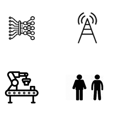
Achronix FPGAs Help Power Industry 4.0 and 5.0 Innovation– Achronix Staff,Sr Manager, Product Marketing and Business DevelopmentAchronix standalone and embedded FPGA IP combining GDDR6 memory, machine learning processors (MLPs) and the revolutionary two-dimensional network on chip (2D NoC) provide the ideal platform to power industry 4.0 and 5.0 innovation. |
> |
|
Achronix Showcases AI FPGA Application at the TSMC Innovation Zone– Alexandra Saavedra,Demand Generation ManagerAchronix will be participating in TSMC's 2023 North America Technology Symposium on April 26 in Santa Clara, California. The symposium is an excellent opportunity to learn about TSMC's advanced technology progress on 7nm, 6nm, 5nm, 4nm, 3nm processes, and beyond. |
> |

|
Achronix Takes on Conversational AI– Achronix Staff,Sr Manager, Product Marketing and Business DevelopmentAchronix Speedster7t FPGAs, enabled by our two-dimensional network on chip (2D NoC) supplying 20 Tbps of bi-directional bandwidth, are uniquely positioned to provide the best performance possible for Conversational AI applications. |
> |

|
Achronix’s Next-Generation, 7nm FPGA Family Will Feature Micron’s Blazingly Fast GDDR6 Memory – To 4 Tbps and Beyond– Manoj Roge,VP of Strategic Planning & Business DevelopmentMicron Technology announced today that its high-performance GDDR6 SDRAM (in volume production since June) will be the high-speed memory of choice for Achronix’s yet-to-be-announced, next-generation FPGA family, making Achronix the world’s first FPGA vendor with announced GDDR6 support. |
> |

|
Autonomous Vehicle Trends and Technology Evolution– Bob Siller,Director, Product MarketingThe value of FPGAs in automotive design has long been established as the technology has been used in over 200 million vehicles over the last 15 years. However, looking beyond the FPGA, it is clear that, for the needs of ADAS today, the eFPGA reigns supreme. |
> |
|
Back to Basics: A Layman’s Introduction to the eFPGA– Alok Sanghavi,Sr. Marketing ManagerTo answer the question of what an embedded field programmable gate array (eFPGA) is, we first have to answer the question of what is an FPGA. To oversimplify. an FPGA is a chip that is able to rewire its internal workings in the field whenever instructed, and then operate at hardware (as opposed to software) speeds until such time as it is rewired again. This capability is known as field programmability. |
> |