High-Speed Interfaces
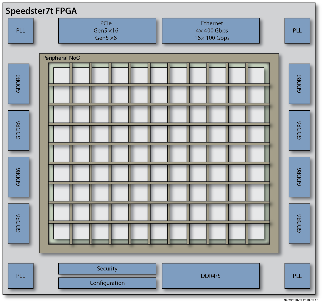
For network-based applications in the data-center, high-speed data enters an FPGA-based processing node in two fundamental ways: through PCIe connections to a host processor and via high-speed Ethernet connections to other data-center resources. The Speedster7t FPGA family is designed to maximize data rates over these connections with a number of PCIe Gen5 interfaces for the host-processor connection and multiple 400G Ethernet connections. Both of these I/O standards represent the fastest, most recent specifications for inter- and intra-system data communications used in data centers and many other FPGA-based applications. Speedster7t FPGAs offer multiple, high-speed I/O ports supporting data rates that data centers expect to see in the near future.
The Speedster7t FPGA family incorporates up to 385 megabits of embedded memory for data that needs to be accessed quickly. However, the amount of data that must be handled by many data center applications almost universally overwhelms these resources. Therefore the Speedster7t FPGAs are designed with up to 8 GDDR6 SDRAM controller ports, providing the fastest SDRAM access speeds with the lowest DRAM cost (per stored bit) and at power levels close to LPDDR5 SDRAM.
Ethernet Support
Speedster7t FPGAs include multiple Ethernet subsystem ports consisting of 8 SerDes lanes and Ethernet MACs to support a combination of applications. The Ethernet MAC is very flexible and can support multiple ports and configurations up to 400G, with each SerDes lane able to achieve a line rate between 10G and 100G. This high performance Ethernet subsystem connects to the FPGA fabric through the 2 dimensional network on chip (2D NoC).
| Mode | Number of Channels | SerDes Rate (Per Lane) | SerDes Lanes |
|---|---|---|---|
| 400G | Up to 2 | 100G | 4 lanes each channel |
| 1 | 50G | 8 lanes | |
| 200G | Up to 2 | 50G | 4 lanes each channel |
| Up to 4 | 100G | 2 lanes each channel | |
| 100G | Up to 2 | 25G or 26.5G | 4 lanes each channel (KR4 or KP4) |
| Up to 4 | 50G | 2 lanes each channel | |
| 50G | Up to 4 | 25G | 2 lanes each channel |
| 10G/25G/50G/100G | Up to 8 | 10G, 25G, 50G, 100G | Independent single-lane applications |
PCI Express
Speedster7t FPGAs have multiple PCIe Gen5 interfaces with 16 lanes (×16) and 8 lanes (×8) configurations. Both PCIe controller interfaces support dual-operation, as either an endpoint or as a root complex.
| Feature | PCIe Port 1 | PCIe Port 2 |
|---|---|---|
| PCI Express Specification | Revision 5.0, Version 0.9 | Revision 5.0, Version 0.9 |
| PIPE | Version 5.1.1 | Version 5.1.1 |
| Maximum width | ×16 | ×8 |
| Maximum throughput | 512 GTs (Gen 5) | 256 GTs (Gen 5) |
| Supported functionality | Root-Port + End-Point | Root-Port + End-Point |
| DMA support | Yes | Yes |
| DMA read channels | 4 | 2 |
| DMA write channels | 4 | 2 |
| BAR | 4 | 4 |
| Virtual channels | 1 | 1 |
| Physical functions | 4 | 2 |
| Virtual functions | 252 | 0 |
| Advanced error reporting (AER) support | Yes | Yes |
| IOV | 256 | None |
GDDR6
GDDR6 SDRAM interfaces are the best choice for next-generation system designs given their combination of high speed and low power. Speedster7t FPGAs contain up to eight GDDR6 interfaces to provide external high-bandwidth memory interface support. Each GDDR6 interface operates on two channels, each of which can be disabled independently.
Each controller supports a wide range of features, including bus utilization optimization, page-hit mitigation, multiport front end (MPFE), reordering and error interrupt. Users can configure the PHY ZQ calibration as master/slave mode across multiple PHY’s. Both the controller and PHY implementation are compliant with the JEDEC GDDR6 SDRAM standard JESD250.
The GDDR6 interfaces can be run up to a data rate of 16 Gbps with device densities from 8 Gb to 16 Gb, supporting up to ×16 in clamshell modes and up to ×8 in non-clamshell modes.
The GDDR6 controller connects to the FPGA fabric via an AXI interface with support for full or half-rate clocking through one of two options:
- A 256-bit AXI interface to the network on chip (NoC), delivering up to 256 Gbps of bidirectional bandwidth
- A 512-bit AXI direct-to-fabric interface, delivering up to 512 Gbps of bidirectional bandwidth
DDR4/5
Speedster7t FPGAs include DDR4 and DDR5 memory interface support for deeper buffering requirements. The PHY and controller are implemented as hard IP and support multiple configurations such as soldered down components on PCB, UDIMM, SODIMM, RDIMM and LRDIMM modules and bit widths from x4 to x72. The interface supports up to 16 ranks and the PHY performs calibration with a microprocessor based training sequence, so the user does not need to worry about the complexity of the design. The PHY and controller support all standard features defined by the JEDEC specification and are inter-operable with memories from all major vendors.