Chiplets Built with Speedcore eFPGA IP
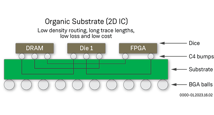
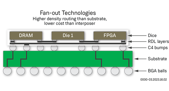
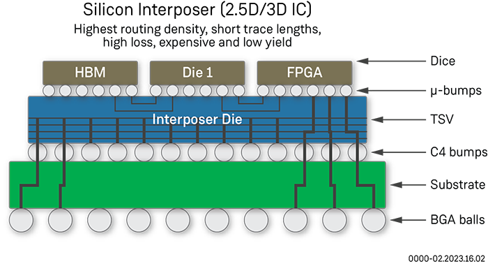
Speedcore™ eFPGA IP can be deployed in various form factors including being integrated into a customer-defined chiplet that can be deployed in a system-in-package (SiP) solution via 2.5D interconnect technology. The following figures show three options for the SiP integration. The first is based on an organic substrate providing the lowest cost but does not provide the highest interconnect density between the die. Redistribution layer (RDL) based interposers are the next step in interconnect density but are also more expensive. Finally, silicon-based interposers provide the most interconnect density and compatibility with high-bandwidth memory (HBM), but come at the highest cost.
Chiplet solutions allow designers to reduce the board space required and realize new integration possibilities compared to a standalone FPGA solution. With a custom Speedcore eFPGA IP-based chiplet solution, designers need to specify the interconnect technology between the chiplet and their ASIC die. Speedcore eFPGA IP is agnostic as to the chiplet interconnect technology and has the interconnect density and performance to work with all the various 2.5D interconnects. Designers can fully customize the amount of logic, DSP blocks, and memory in the Speedcore eFPGA to match their application requirements.
Speedcore eFPGA Chiplet SiP Examples
Benefits of Chiplets with Speedcore eFPGA IP vs. Bare FPGA Die Integration
Traditionally, designers who wanted to develop an integrated ASIC and FPGA solution were required to purchase bare die from an FPGA supplier, but there are challenges to this approach:
- FPGA suppliers do not typically support bare die business because it requires custom processing and testing
- Standalone FPGAs typically do not have the I/O structures required for system-in-package integration
- Standalone FPGAs are not optimized for these types of applications, which leads to excessive power, larger packaging requirements and inter-die bandwidth limitations
On the other hand, by using a chiplet built with Speedcore eFPGA IP, designers can realize benefits such as:
- Lower power and cost by only including the specific and required functionality for their application
- Optimized interfacing between the chiplet and ASIC for maximum bandwidth with minimal latency
- Smaller form-factor packaging based on a size-optimized eFPGA IP chiplet
Benefits of Speedcore eFPGA IP Chiplets vs. Monolithic eFPGA and ASIC Integration
Designers looking for the highest level of integration can choose to develop a monolithic ASIC (single die) which includes Speedcore eFPGA IP. However, in some applications the monolithic integration does not allow for product flexibility that is possible with a chiplet-based approach.
By using an eFPGA IP-based chiplet, designers can realize benefits vs. a monolithic eFPGA ASIC solution, such as:
- Companies can create unique product solutions (different SKUs) without the FPGA chiplet that have lower cost and lower power in the cases where FPGA flexibility is not required.
- Support different process technologies in the cases where the optimal process technology for the ASIC is not optimal for an embedded FPGA. Examples are ASICs built with mixed-signal technology or ASICs built on technology where the eFPGA IP is not available.
Getting Started with Speedcore eFPGA IP Chiplets
The design process used to develop Speedcore eFPGA IP chiplets is the same as developing an ASIC with embedded Speedcore eFPGA IP. This proven design flow makes it easy to develop a Speedcore eFPGA IP chiplet solution that leverages established tools and processes. To get started with Speedcore eFPGA based chiplets, contact Achronix today.