| Blog Icon | Blog Title | |
|---|---|---|

|
Why the Inclusion of Achronix in the Artificial Analysis Report Matters for LLM InferenceThe AI market is entering a new phase. For the past several years, attention has centered on models: larger models, smarter models, and faster-moving model releases. As enterprises and service providers move from experimentation to production, the focus is shifting. |
> |

|
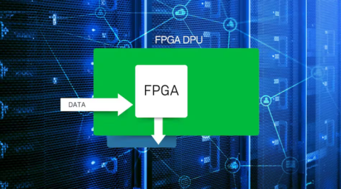
Five Architectural Reasons Why FPGAs Are the Ultimate AI Inference EnginesAs artificial intelligence (AI) models grow more complex and pervasive, the industry continues to grapple with finding the most effective hardware to meet the evolving needs of AI inferencing. While GPUs, TPUs, and CPUs have traditionally handled various AI workloads, FPGAs — especially when backed by high-performance architectures such as Achronix Speedster7t FPGAs — offer unmatched advantages in flexibility, efficiency, and real-time performance. |
> |

|
Achronix and BigCat Wireless Collaborate for 5G/6G WirelessDiscover how Achronix Speedster7t FPGAs, paired with BigCat Wireless DSP IP, deliver groundbreaking performance for 5G/6G networks with enhanced MIMO, beamforming, and real-time processing capabilities. Explore advanced machine learning processors, optimized DSP kernels, and scalable solutions for future wireless technologies. |
> |

|
Achronix Achieves up to 300% Improvement in SoC Verification Times with Synopsys CloudHow Achronix accelerated SoC physical verification times by up to 300% using Synopsys Cloud. Learn about innovative solutions and improved productivity in our latest blog post. |
> |
|
Networking Game Changer: The Potential of SmartNICs with Achronix FPGAsExplore the transformative power of Achronix FPGAs in SmartNIC technology. Discover how composable SmartNICs redefine networking with unparalleled adaptability and performance. Read our latest article on Electronic Design's TechXchange.
|
> |
|
Accelerating LLM Inferencing on FPGAsHow do Speedster7t FPGAs stack up against GPU solutions when running the Llama2 70B parameter model? The evidence is compelling — Achronix Speedster7t FPGAs outperform in processing LLMs by delivering an optimal combination of computational power, memory bandwidth, and exceptional energy efficiency. |
> |
|
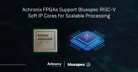
Enabling Scalable Processing with Achronix FPGAs and Bluespec's RISC-V Soft ProcessorsAchronix Semiconductor and Bluespec, Inc. have unveiled a highly scalable suite of Linux-capable RISC-V soft processors specifically designed for the Achronix Speedster7t FPGA family. |
> |
|
Maximizing Data Conversion Efficiency: A Deep Dive Into the Achronix JESD204C SolutionDiscover Achronix's cutting-edge JESD204C solutions on Speedster7t FPGAs, offering high-speed data converter interfaces for your custom ADC/DAC designs. Learn about increased lane rates, robust links, and more. Request a free demo now! |
> |

|
What’s New in FPGAs at Achronix: A Q&A With EDACaféOur VP of Marketing, Steve Mensor, recently sat down with the team from EDACafé to talk about what's new in the world of Achronix. Read on to see the highlights of Steve's recent Q&A session. |
> |