Achronix has a long history of delivering innovations and pushing the boundaries in high-performance FPGA applications, often in data-intensive and high-bandwidth applications across different industries. Some of these applications require interfacing with advanced analog-to-digital converters (ADC) and digital-to-analog converters (DAC) — a mission best accomplished with JESD204C.
JESD204B/C is a high-speed data converter serial interface standard defined and developed by JEDEC. The standard reduces the number of data inputs and outputs between high-speed data converters and other high-performance devices, such as Achronix Speedster7t FPGAs. This combination of digital and analog signal chains benefits designers by allowing them to have a simplified and small form-factor board layout without adversely affecting the performance of the end system. The interface/interconnect between the data conversion devices is via high-speed general-purpose I/O (GPIO) or SerDes lanes.
Achronix has implemented a JESD204C interface on its Speedter7t FPGAs to enable customers to work with the ADC/DAC of their choice. Customers can use their preferred ADC/DAC devices and customize their design owing to the soft implementation of a JESD204C interface on a homogeneous FPGA architecture. This blog discusses JESD204C solutions available on Achronix Speedster7t FPGAs.
The Achronix JESD204C solution supports all the outlined features and suggested improvements over the previous versions. It aims to address all of the four goals put forth by the standards body:
- Increased lane rates to support the higher total bandwidth needed — Achronix solutions currently support data rates up to 24.75 Gbps per SerDes lane. The SerDes can support the JESD204C upper limit lane rates of 32 Gbps. The data converter for testing the design was the Analog Devices AD9082, which supports a maximum data rate of 24.75 Gbps.
- Improved payload delivery efficiency — Achronix users can customize and optimize their designs using the FPGA fabric.
- Link robustness — Achronix solutions demonstrate highly robust links in single- and multi-channel modes while maintaining deterministic latency. For example, the sample rates can go up to the highest limits supported by AD9082 for those modes without quantization effects.
- Backwards compatibility with the previous JESD204B version — An Achronix JESD204B implementation is in the roadmap.
Lab Tested Solution
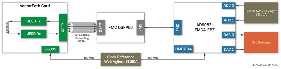
Achronix has successfully implemented and demonstrated the Speedster7t JESD204C reference solution interfacing to the Analog Devices AD9082, quad 16-bit DAC, dual 12-bit ADC device. The lab loop-back setup (shown in figure 1) includes the following components:
- VectorPath 815 Board with Speedster7t FPGA.
- VectorPath-to-ADI EVAL-AD9082 connector board. Achronix has developed a 4-lane QSFP to FMC connector, which can be modified for 8 or 16 lanes, if necessary.
- ADI EVAL-AD9082 ADC/DAC board with FMC connector.
- Required test equipment and accessories.
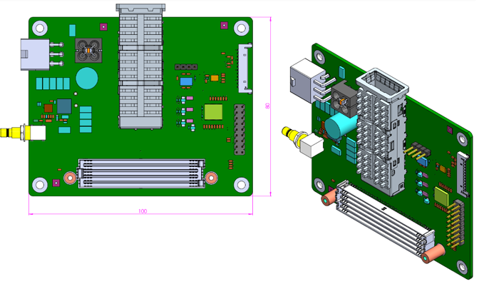
VectorPath-to-ADI EVAL-AD9082 Connector Board
The lab setup allows for a complete signal chain in both transmit (Tx) and receive (Rx) directions. The function of individual components is as follows:
- JESD204C transmit/receive IP are implemented in the Speedster7t AC7t1500 FPGA on the VectorPath card. Particular test scripts are run via a Linux console on the attached PC.
- The Speedster7t SerDes channels are connected to the ADC/DAC via a custom FMC-QSFP connector board. The QSFP28 module allows support for four SerDes lanes, each running at 24.75 Gbps.
- The programming of the thousands of ADI AD9082-FMCA-EBZ evaluation board registers is accomplished with API calls issued by a connected PC. Alternatively, registers can be programmed using a soft CPU core on the FPGA or a hard CPU core in an SoC.
- An external clock source synchronizes both the VectorPath card and the AD9082-FMCA-EBZ evaluation board. Internal clocks can also be generated using the oscillator on the AD9082-FMCA-EBZ and fed to the VectorPath card via an FMC-QSFP connector.
- An arbitrary waveform generator (AWG) generates the input waveform fed externally through to ADC0 and ADC1.
- Loop-back happens inside Speedster7t FPGA between the JESD204C receive and transmit blocks, while the DAC output is displayed on an oscilloscope.
- Expected waveforms at the outputs of DAC0 and DAC1 are displayed on the attached oscilloscope.
Four Lane-Loopback Example
The preceeding diagram shows a four-lane loopback configuration. The signal path is AWG (I/Q Signal) → AD9082-FMCA-EBZ (ADC) → FMC QSFP56 → Speedster7t JESD204C Rx → Loopback → Speedster7t JESD204C Tx → FMC QSFP56 → AD9082-FMCA-EBZ (DAC) → Oscilloscope.
The input I/Q waveforms to ADC0 and ADC1 of AD9082-FMCA-EBZ have the same frequency but are phase-shifted by 90°. The frequency depends on the supported modes for the AD9082-FMCA-EBZ and the setup can achieve the highest frequency listed for that particular mode with minimal and acceptable jitter.
The state-of-the-art Achronix JESD204C solution on the Speedster7t FPGA can achieve the highest rate supported by JESD204C data converters. The solution enables a vendor-agnostic interface with the connected ADC/DAC devices, allowing customers to deploy with their preferred vendor(s).
Contact our experts to request a free demonstration or evaluation.