Achronix Speedster7t FPGAs feature a revolutionary new two-dimensional network on chip (NoC), which provides >20 Tbps ultra-high bandwidth connectivity to external high-speed interfaces and for routing data within the programmable logic fabric. The NoC is structured as a series of rows and columns spread across the Speedster7t FPGA fabric. Each row or column has two 256-bit data paths using industry standard AXI data format, which support 512 Gbps data rates. For more details on the Speedster7t NoC, visit Revolutionary New 2D Network-on-Chip.
The Speedster7t FPGA NoC offers several important advantages for FPGA design including:
- Improves design performance
- Reduces the risk of place-and-route congestion in designs with high logic utilization
- Reduces power consumption
- Simplifies logic design by replacing traditional logic data routing with the NoC
- Enables modular FPGA design
This blog uses a specific FPGA design example to show the important role played by the NoC to increase performance and reduce routing congestion in the FPGA fabric. This design implements a triple data encryption and decryption algorithm (3DES). It applies the 3DES encryption algorithm three times for each data block and increases the security by increasing the 3DES key length.
In this FPGA design, we place the input and output pins in four locations on the top, bottom, left, and right side of the FPGA. The data coming from the top pin is decrypted by logic 1, then sent to logic 2 via the blue traces to be encrypted, and transmitted via the bottom pins. The data coming in from the left pins are decrypted by logic 3, then sent to logic 4 through the red trace to be encrypted and transmitted out to the right pins.
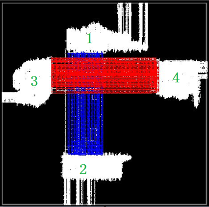
3DES FPGA Design Layout Diagram (Without NoC)
If implemented in a tradition FPGA architecture, the problems encountered with this design are as follows:
- The routing connecting the encryption and decryption modules in the middle of the FPGA are congested.
- To maintain design performance, there needs to be an increase in the number pipeline registers.
- Since the connection bus is 256 bits wide, adding several stages of pipeline registers will consume a lot of register resources.
- The crossover point between the connected modules (1,2,3 and 4) is very congested. As the design complexity increases, the design may not route or the performance may degrade due to routing delays encountered by routes detouring around the congested areas.
The above problems are typical for FPGA designers building complex FPGA designs: design complexity, limitations of the hardware platform, and designs having to be connected to peripherals in different fixed locations due to needing to connect to hard IP within the FPGA.
The use of the Speedster7t NoC solves the congestion problem in a way not possible before with previous FPGA architectures. The NoC provides a bidirectional logical interconnect of 288 bits when configured in the data streaming mode. Users can perform logical direct connections or custom protocol interconnection through these 288-bit paths.
Internal Logic Interconnection Using 2D NoC
Speedster7t FPGAs offers 80 master and 80 slave network access points (NAPs) distributed throughout the FPGA core to connect functions in the FPGA fabric to the NoC. The designer simply instantiates the NAP primitives or macros to connect the logic to the NoC.
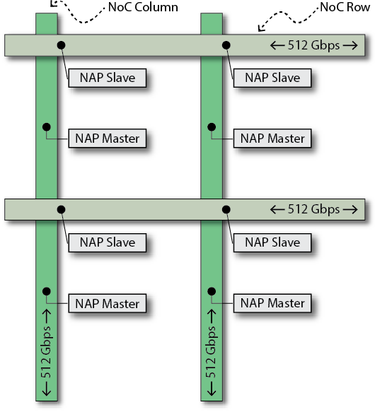
Speedster7t NoC Rows, Columns and Network Access Point (NAP)
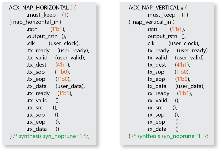
Instantiation of NAP Macros Example
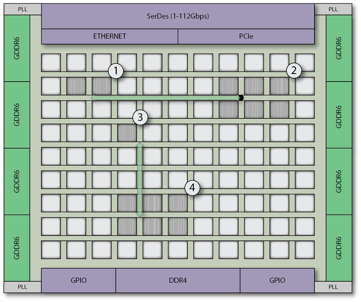
Using the NoC greatly simplifies the 3DES design floorplan, and very importantly, increases the design performance from 260 MHz to 750 MHz, a staggering 188% increase. The figure below shows that the large number of connection buses between logic modules are no longer visible. The bus connections have been absorbed into the NoC and only the green clock traces and the logic traces inside the white module are visible.
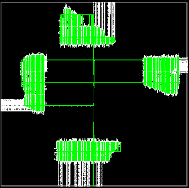
Internal Logic Interconnection Using 2D NoC
In this blog, we shared how FPGA designers can take advantage of the Speedster7t NoC to connect between the internal logic of the Speedster7t FPGA compared to using traditional logic bus routing where performance cannot easily be improved. Not only do we gain a huge increase in performance, but also save time in the design process when integrating different FPGA IP modules.
Stay tuned for more articles, reference designs and technical insights on the Speedster7t NoC.