Once you’ve made the correct decision to add Speedcore eFPGA IP to your ASIC or SoC design, the next question you’ll need to answer is how large to make the eFPGA. That’s a multi-dimensional question because Speedcore eFPGAs contain many types of blocks including:
- LUTs – grouped together in reconfigurable logic blocks (RLBs) along with MUXes, registers, and 4-bit ALUs
- BRAMs – dual-ported, 20Kb block RAMs
- LRAMs – single-ported, 4Kb logic RAMs
- DSP64 math units
You’ll need to decide how many of each type of block you’ll need to implement your application(s) within your overall ASIC or SoC design. Once you make those decisions, Achronix uses a tool called Speedcore Builder to give you details about your Speedcore instance including final resource counts for each type, number of I/O, die size with dimensions, static power consumption, configuration time, and test time. Any of the dimensions can be changed in Speedcore Builder until you have the Speedcore instance that meets your exact requirements. A typical Speedcore instance looks something like this:
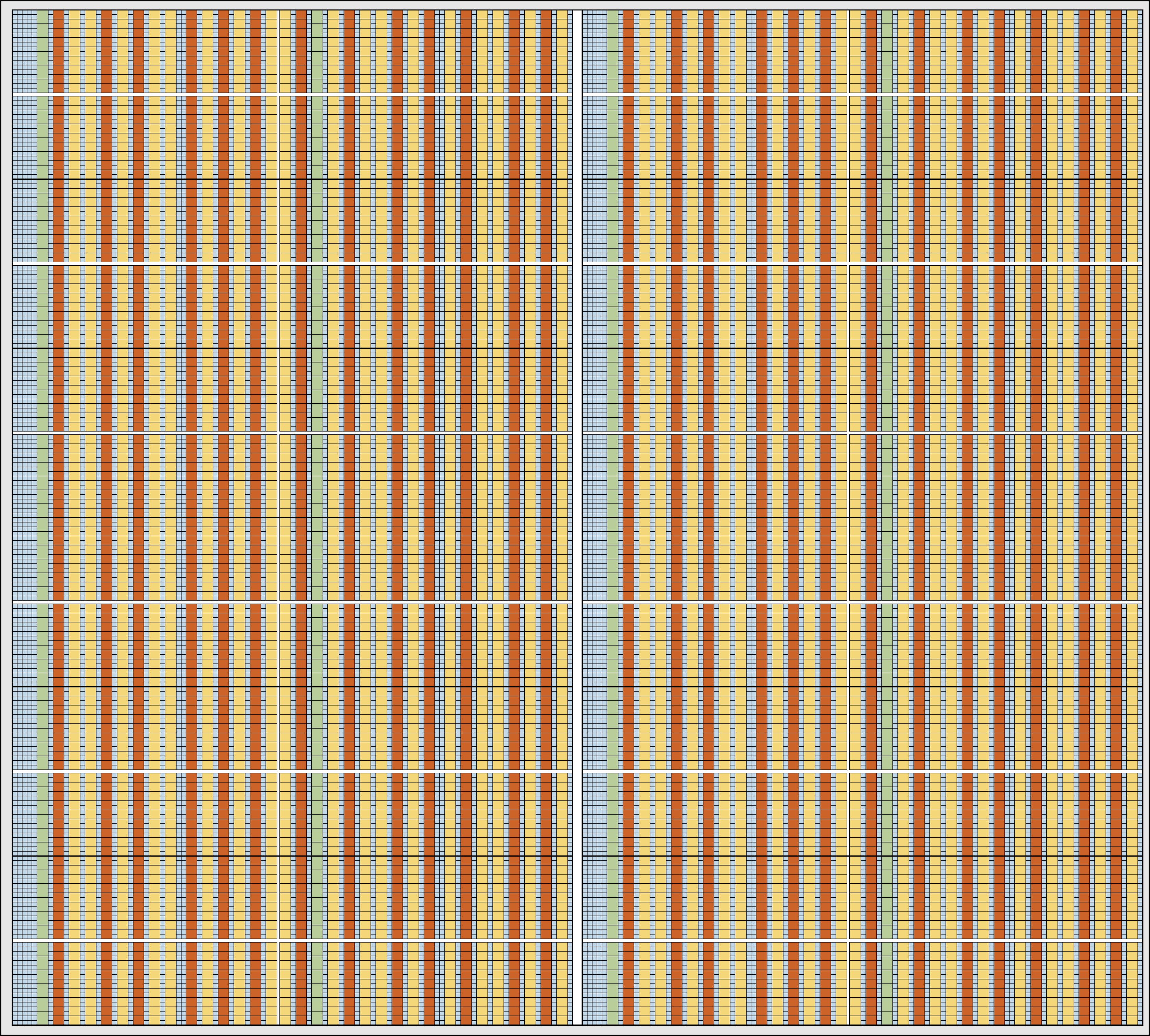
Typical Speedcore eFPGA IP Core (200k LUTs, 17 MB, 3.8k DSPs)
But how do you make these design decisions and how do you resource your Speedcore eFPGA core?
You certainly don’t want to undersize or under resource the Speedcore instance because an overly small eFPGA might be unable to accommodate your largest acceleration tasks. You also don’t want to oversize the eFPGA core because it will consume more silicon real estate than needed. You want a happy medium with enough margin to handle the unexpected (because the unexpected always occurs).
You also want to ensure that your choices provide the right mix of resources for your application needs. This is one of the many advantages of using an Achronix Speedcore eFPGA: You determine the right mix of FPGA resources for your specific application. Perhaps your applications require more DSP64 blocks or more BRAM blocks. You are free to make those decisions when you’re defining your own eFPGA.
So Just How do You Decide?
There are three main ways that Speedcore eFPGA users make these decisions, depending on their requirements and prior experience.
Exiting Standalone FPGA Users
Users of standalone, packaged FPGAs with existing designs will already have a collection of design files that can be used to help define the resource count for their eFPGA. These users may wish to convert a design from using a standalone FPGA to an eFPGA in their ASIC or SoC to improve overall system performance by eliminating long-latency, chip-to-chip communications or to take advantage of one of the other Speedcore eFPGA benefits. (See “When, Why, and How Should You Use Embedded FPGA Technology for Hardware Acceleration?” for a list of these additional benefits.) It’s much easier to estimate the number and types of resources a programmable-logic design will require when you already have a design in hand
You can use the resource numbers from the existing design as instantiated in the existing FPGA; however, a better and more accurate approach is to port that design to the Achronix ACE design tools, synthesize it, and let the ACE design tools generate the resource counts for you. However, you need to make sure you have enough resources for a realistic design cycle. In other words, add some margin to the resource count so you don’t get caught short.
ASIC Users with Existing Logic
Some Achronix customers want to port an existing application design from ASIC gates into programmable logic to gain additional flexibility as a means of future-proofing their design — either to accommodate changing standards or new market requirements as they occur. If a design is already implemented in ASIC gates, then the amount of logic, memory, and other resources are known quantities. However, there are a couple of traps on this path that you will want to avoid.
The first trap is to think you can make a simple, one-to-one conversion from ASIC gates to programmable-logic resources using a single “equivalent gates” calculation. It’s much better to port the design to the Achronix ACE tools to get an accurate resource estimate. The second trap is a performance trap. Programmable logic simply is not as fast as hard ASIC logic. The abundant on-chip switching and multiplexing that gives programmable logic its flexibility extracts a performance cost. However, you can regain performance shortfalls by widening data paths, adding parallel execution units, adding pipeline registers, and optimizing state machines.
ASIC Users with Just Ideas
Other Achronix customers simply do not know where to start but they want to investigate the possibilities. They don’t have a design in hand, don’t know if they might be able to use an eFPGA or what their programmable-logic needs will be. They haven’t thought about how they want to use a Speedcore eFPGA to add flexibility to and future-proof their ASIC or SoC. In these cases, customers work closely with Achronix to narrow the possibilities. Even without a specific application design in hand, these customers may have benchmark designs that resemble the intended application. These benchmark designs are useful as a starting point.
If you have additional questions or would like to discuss how your ASIC or SoC design can benefit from an on-chip eFPGA, or if you would like some help to determine just how much eFPGA your design needs, please contact Achronix directly.