As the world continues its journey into a complete digital transformation, the way that data gets collected, processed and stored is changing dramatically. Approximately 328.77 million terabytes of data are created each day. It is estimated that the world will create more than 175 zettabytes of data per year by 2025. Smart phones, smart cities, autonomous vehicles, artificial intelligence, telemedicine, artificial reality, virtual reality, gaming and so many more use cases are the driving force behind this tsunami of data.
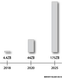
Annual Worldwide Data Production
When cloud computing originated, the idea was to stack up relatively inexpensive, generic 1-socket and 2-socket servers to take on the various workloads and as the demand increased, the data center would simply add more server nodes. As data centers grew to 10’s, if not 100’s of thousands of server nodes, it became clear that the power to run and cool these machines and the real estate needed to house them became cost prohibitive.
In an attempt to make the server nodes more efficient, unbeknownst to the wider market, a new sub-class of semiconductor product started evolving… the data accelerator. One of the earliest forms of a data accelerator was the repurposing of the Graphic Processing Unit (GPU), which is ideal for processing large data sets. GPUs found their way into parallel processing, SQL data base calculation, image recognition, big data analytics and artificial intelligence in the core data center.
Beyond the compute hurdles was a need to move data very quickly. Modern data centers are architected with distributed compute and storage resources which require sophisticated networking capabilities. As with the compute workloads, the generic servers were being overwhelmed with the processing of packets and managing traffic engineering instead of focusing on application workloads. The generic Ethernet NIC evolved into a SmartNIC in many of these use cases and has continually gained in popularity in the data center. These data accelerators are used to create many of these networking and storage acceleration solutions including network overlays, kernel bypass solutions, deep packet classification, capture and telemetry just to name a few. FPGAs have been established as one of the key enablers of SmartNICs due to the gate-level speed and complete flexibility.
Yet another paradigm shift has been underway in recent years which is decentralizing the core data center and moving applications and workloads to the edge of the network. Multi-access edge computing (MEC) moves the compute and storage of many applications traditionally processed in the core data center to the edge network where space, power and cost requirements are very tight. Many applications such as autonomous vehicles, gaming and telemedicine will be dependent on ultra-low latency (sub-20ms) latencies which simply cannot be attained using the core data center. Data accelerators will need to meet very stringent cost and power profiles, maintain flexibility and deliver much needed performance.
Beyond the two previously-mentioned data acceleration solutions, GPUs and FPGAs, there is a third approach to data accelerators which is custom ASICs. Although custom ASICs will always provide the highest performance with the least amount of power, ASICs suffer from being a fixed solution. Once designed, a bug in the design, a change in the application specification, a new machine learning model or desired change in application altogether takes away all of the benefits that an ASIC brings.
GPUs, which have been proven useful for processing heavy data sets, are plagued by excessive power and generally shorter life expectancy. They also do not provide the comprehensive flexibility to cover all requirements for networking and storage acceleration use cases. With the programmability of a CPU or GPU and the speed of an ASIC, FPGAs offer the optimal efficiency of power and performance when flexibility is a requirement for compute, networking and storage acceleration use cases. Modern FPGAs provide a mix of hardened IP cores for features such as high speed Ethernet, PCIe, memory and various internal functional blocks and the FPGA fabric itself. This provides a balance of flexibility where you need it and lower power and cost for the fixed functionality.
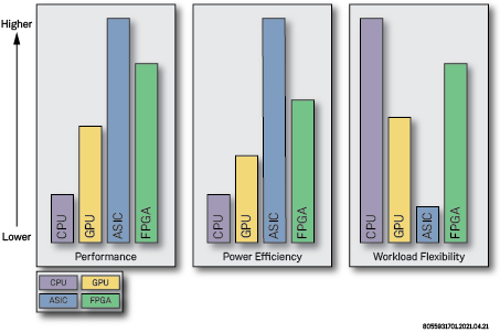
CPU vs GPU vs ASIC vs FPGA
Achronix, a market leader in high-end FPGA technology, sets itself apart from the competition in two ways; 1) offering the highest bandwidth FPGA in the industry and 2) being the only high-end FPGA vendor to offer eFPGA intellectual property (IP). Manufactured at TSMC, Speedster®7t is Achronix’s flagship, 7nm FPGA family touting 400GbE, PCIe Gen 5, GDDR6, DDR4, machine learning processors (MLPs) and an industry changing 2-dimensional network on chip (2D NoC) with bi-directional bandwidth exceeding 20 Tbps. Speedcore™ eFPGA IP enables users to receive the FPGA logic, memory, MLPs and 2D NoC as intellectual property for integration in their ASIC/SoC. Use cases include custom ASICs as well as chiplets for various multi-chip module SoC solutions. Whether for development purposes or a final product, Achronix through its partnership with Bittware, offers the VectorPath® accelerator card based on the Speedster7t FPGA. All three of these solutions from Achronix are supported with a single tool chain known as the Achronix tool suite.
To learn more about our latest FPGAs, please contact Achronix and visit the Speedster7t pages on Achronix.com.