Each instance of an Achronix Speedcore eFPGA in your ASIC or SoC design must be configured after the system powers up because Speedcore eFPGAs employ nonvolatile SRAM technology to store the eFPGA’s configuration bits. Each Speedcore instance contains its own FPGA configuration unit (FCU) that initializes, configures, and manages the Speedcore eFPGA’s core logic array. For example, if you instantiate three Speedcore eFPGAs in your ASIC/SoC design, there will be three FCUs on the chip. Each FCU has a set of configuration pins and a set of configuration-mode pins that help to determine how the configuration pins will operate.
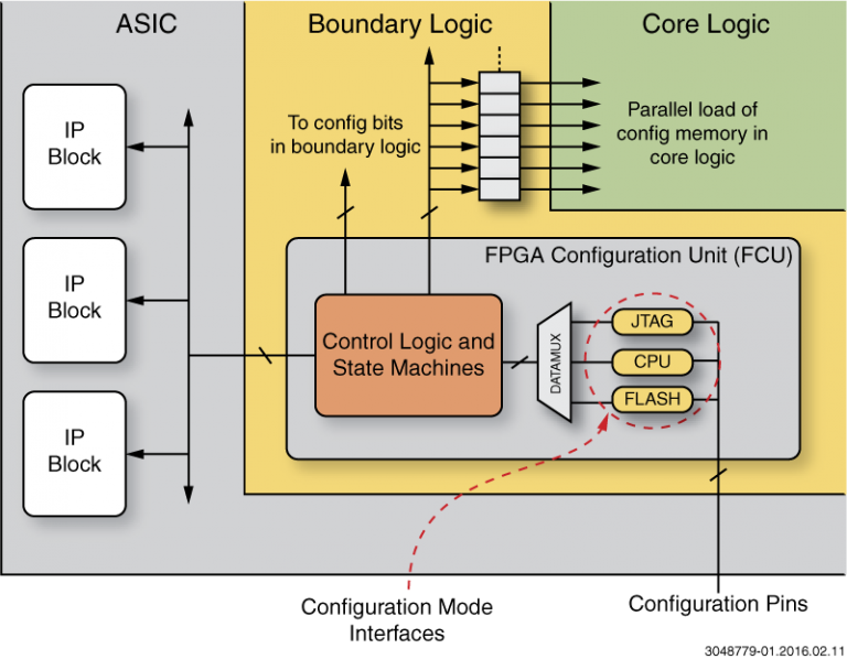
The figure below shows the relationship among the ASIC/SoC, the Speedcore eFPGA’s boundary logic including the FCU, and the Speedcore eFPGA’s core logic:
As the figure above shows, the FCU’s configuration-mode pins feed three mode-dependent blocks marked JTAG, CPU, and Flash—which are the three types of configuration interfaces available in the FCU. The FCU’s configuration-mode pins along with a register-based setting in the eFPGA’s JTAG controller determine how the configuration pins operate.
The configuration-mode pins alone can select between the CPU and Flash modes. However, the JTAG configuration mode is independent of the configuration-mode pins. JTAG mode is enabled by sending FCU commands that set the appropriate bits in the Speedcore eFPGA’s JTAG TAP controller. Once JTAG mode is enabled, it overrides the settings of the configuration-mode pins until disabled. This organization allows the JTAG controller to take control of the eFPGA regardless of the configuration-mode settings.
Each of these three configuration modes offers unique advantages.
CPU Configuration Mode
The FCU’s CPU configuration mode allows an external CPU to act as a master to control the programming operations for the Speedcore eFPGA, which acts as a slave in this mode. The CPU mode operates over a 1-, 8-, 16-, 32-, or 128-bit wide parallel interface.
CPU mode is the Speedcore eFPGA’s fastest possible configuration mode because it permits the eFPGA’s configuration bitstream to enter the FCU over a 128-bit bus (in its widest configuration) at the maximum supported clock rate. All Speedcore eFPGA configuration modes support a 100 MHz maximum clock rate, so the maximum bitstream configuration data rate in the CPU configuration mode is a brisk 12.8 Gbits/sec.
Serial Flash Configuration Mode
The FCU’s Speedcore eFPGA’s Serial Flash configuration mode allows the FCU to load configuration bitstreams from SPI serial NOR flash memories. In this mode the eFPGA is the master and supplies the clock to the SPI flash memory. As with the CPU configuration mode, the Serial Flash configuration mode’s maximum clock rate is 100 MHz. However, not all serial flash devices can operate at 100 MHz. To accommodate this potential limitation, the FCU can drive the flash memory’s clock at three additional clock rates derived from the clock supplied by the ASIC/SoC to the FCU. The four available clock rates for the serial Flash memory are:
- Divide by 1 (full speed)
- Divide by 2
- Divide by 4
- Divide by 8 (default)
You select the clock rate when generating the configuration bitstream using Achronix’ ACE design tools. Selection is configured using the ‘Serial Flash Clock Divider’ drop-down menu in the ‘Bitstream Generation Implementation Options’ section of the ACE GUI. Initially at power up, the FCU’s Serial Flash configuration mode operates with a divide-by-8 flash clock because it’s the safest clock rate, compatible with any flash memory device. An FCU command embedded early in the configuration bitstream can then increase the flash memory’s clock rate as set by the ACE tools to decrease the overall configuration time while loading the configuration from the serial flash memory.
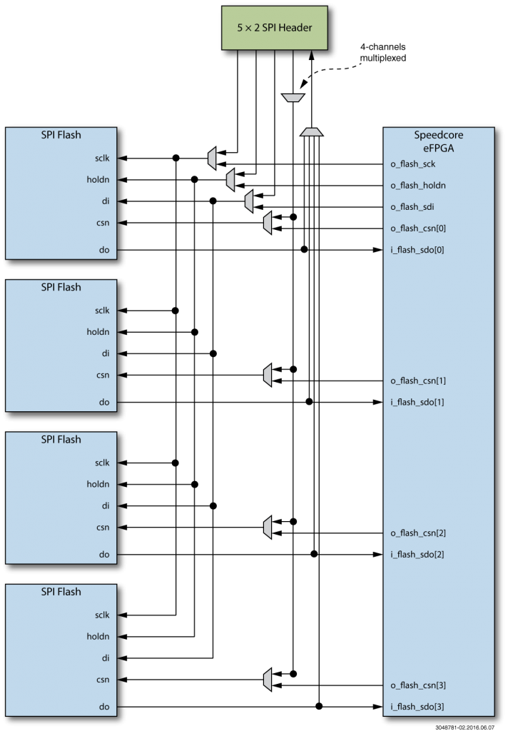
The Speedcore eFPGA’s Serial Flash mode is designed for use with 1-bit-wide flash devices. It is also possible to operate in a 4-bit mode that accepts one bit from each of four 1-bit-wide flash devices (as shown in the figure below), which results in faster configuration times and permits the storage of larger configuration bitstreams.
JTAG Configuration Mode
The FCU’s JTAG configuration mode employs the Speedcore eFPGA’s JTAG Tap controller, which complies with IEEE Std 1149.1. Because the Speedcore JTAG implementation is used for bitstream programming as well as for real-time, in-system control and observation, the JTAG TAP controller is allowed to take control of the FCU upon receipt of the appropriate data register (DR) command, regardless of the eFPGA’s configuration-mode pin settings.
When set to JTAG configuration mode using a JLOAD DR instruction, the Speedcore TAP controller accepts configuration data supplied by the JTAG port on the ASIC/SoC’s JTAG TDI data-input pin and converts it into instructions for the JTAG logic within the FCU. The JTAG logic in the FCU uses these DR instructions to assemble standard 128-bit Speedcore configuration frames, which are then forwarded to the FCU state machines that load the eFPGA’s configuration memory and configure the eFPGA’s core logic.
Although the Speedcore JTAG port can operate at a maximum 100 MHz clock rate like the eFPGA’s other configuration modes, the JTAG configuration mode is the slowest of the three configuration modes because it is a 1-bit interface plus the substantial communications overhead bits added to the configuration bitstream to conform to JTAG instruction protocols.
Note: Part 2 of this blog series will discuss configuration programming times using the three Speedcore eFPGA configuration modes.
For more in-depth Achronix’ Speedcore eFPGA configuration techniques including ways to connect multiple Speedcore eFPGA cores to one CPU core on ASIC/SoC, bitstream encryption features, and CRC error checking, download the Speedcore Configuration User Guide (UG061).


