| Blog Icon | Blog Title | |
|---|---|---|
|
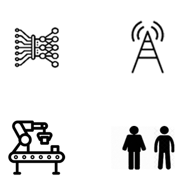
Achronix FPGAs Help Power Industry 4.0 and 5.0 Innovation– Achronix Staff,Sr Manager, Product Marketing and Business DevelopmentAchronix standalone and embedded FPGA IP combining GDDR6 memory, machine learning processors (MLPs) and the revolutionary two-dimensional network on chip (2D NoC) provide the ideal platform to power industry 4.0 and 5.0 innovation. |
> |

|
Achronix Showcases AI FPGA Application at the TSMC Innovation Zone– Alexandra Saavedra,Demand Generation ManagerAchronix will be participating in TSMC's 2023 North America Technology Symposium on April 26 in Santa Clara, California. The symposium is an excellent opportunity to learn about TSMC's advanced technology progress on 7nm, 6nm, 5nm, 4nm, 3nm processes, and beyond. |
> |

|
Achronix Takes on Conversational AI– Achronix Staff,Sr Manager, Product Marketing and Business DevelopmentAchronix Speedster7t FPGAs, enabled by our two-dimensional network on chip (2D NoC) supplying 20 Tbps of bi-directional bandwidth, are uniquely positioned to provide the best performance possible for Conversational AI applications. |
> |

|
Achronix’s Next-Generation, 7nm FPGA Family Will Feature Micron’s Blazingly Fast GDDR6 Memory – To 4 Tbps and Beyond– Manoj Roge,VP of Strategic Planning & Business DevelopmentMicron Technology announced today that its high-performance GDDR6 SDRAM (in volume production since June) will be the high-speed memory of choice for Achronix’s yet-to-be-announced, next-generation FPGA family, making Achronix the world’s first FPGA vendor with announced GDDR6 support. |
> |

|
Autonomous Vehicle Trends and Technology Evolution– Bob Siller,Director, Product MarketingThe value of FPGAs in automotive design has long been established as the technology has been used in over 200 million vehicles over the last 15 years. However, looking beyond the FPGA, it is clear that, for the needs of ADAS today, the eFPGA reigns supreme. |
> |
|
Back to Basics: A Layman’s Introduction to the eFPGA– Alok Sanghavi,Sr. Marketing ManagerTo answer the question of what an embedded field programmable gate array (eFPGA) is, we first have to answer the question of what is an FPGA. To oversimplify. an FPGA is a chip that is able to rewire its internal workings in the field whenever instructed, and then operate at hardware (as opposed to software) speeds until such time as it is rewired again. This capability is known as field programmability. |
> |
|
Benefits of Using FPGA and eFPGA IP in your Design– Bob Siller,Director, Product MarketingWhile FPGAs have been around for over 30 years, eFPGA IP is a relatively new technology that is now finding its way into high-volume applications. Modern eFPGA IP support the same 7nm process technology as high-performance standalone FPGAs. |
> |

|
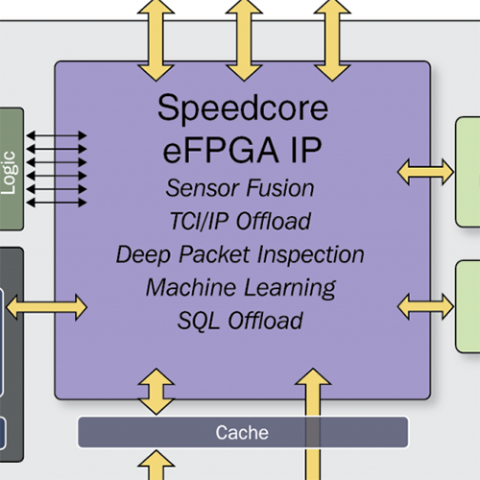
Check out our Recent Video on the Basics of eFPGA Acceleration– Alok Sanghavi,Sr. Marketing ManagerOur existing customers ask us some pretty big questions: “How can this technology implement a step-change in my specific process? How can Speedcore IP be integrated in my SoC? How can you increase the performance of my ASIC?” We revel in answering such questions. However, when we first meet with a company interested in our embedded FPGA (eFPGA) IP, often the question is very simply, “At the most basic level, what can it do for me?” This question may be the most important one we’ll ever answer for them. |
> |
|
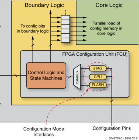
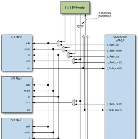
Configuring your Speedcore eFPGA, Part 1: Configuration Interfaces– Volkan Oktem,Sr. Director of ApplicationEach instance of an Achronix Speedcore eFPGA in your ASIC or SoC design must be configured after the system powers up because Speedcore eFPGAs employ nonvolatile SRAM technology to store the eFPGA’s configuration bits. Each Speedcore instance contains its own FPGA configuration unit (FCU) that initializes, configures, and manages the Speedcore eFPGA’s core logic array. For example, if you instantiate three Speedcore eFPGAs in your ASIC/SoC design, there will be three FCUs on the chip. |
> |
|
Configuring Your Speedcore eFPGA, Part 2: Configuration Time– Volkan Oktem,Sr. Director of ApplicationAs discussed in part 1 of this blog post, each instance of an Achronix Speedcore eFPGA in your ASIC or SoC design must be configured after the system powers up because Speedcore eFPGAs employ nonvolatile SRAM technology to store its configuration bits. The time required to program a bitstream into a Speedcore eFPGA depends on the configuration mode being used, the data width, clock frequency, and of course, the size of the configuration bitstream. |
> |